Here is a quick demo on how to load a true type font in Retro Studio.
Creating an analogue watch face in Retro Studio
WatchBlox Tetris Clone!

Retro Studio Private Alpha

Retro Screen!
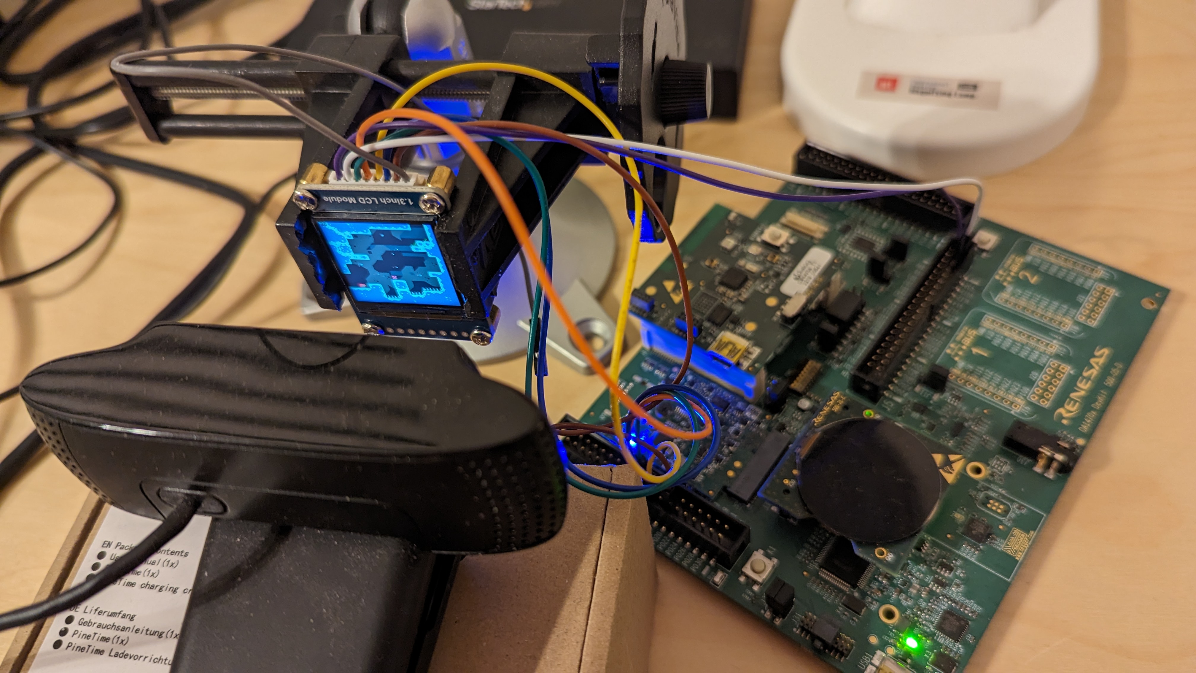
Custom LCD + glass ordered, LCD driver working, it looks so nice compared to the old 240x240 tft (video doesnt do it justice).
At first I was annoyed at not being able to find a square display... but this slight widescreen with the rounded corners gives it a definite TV look and that is great
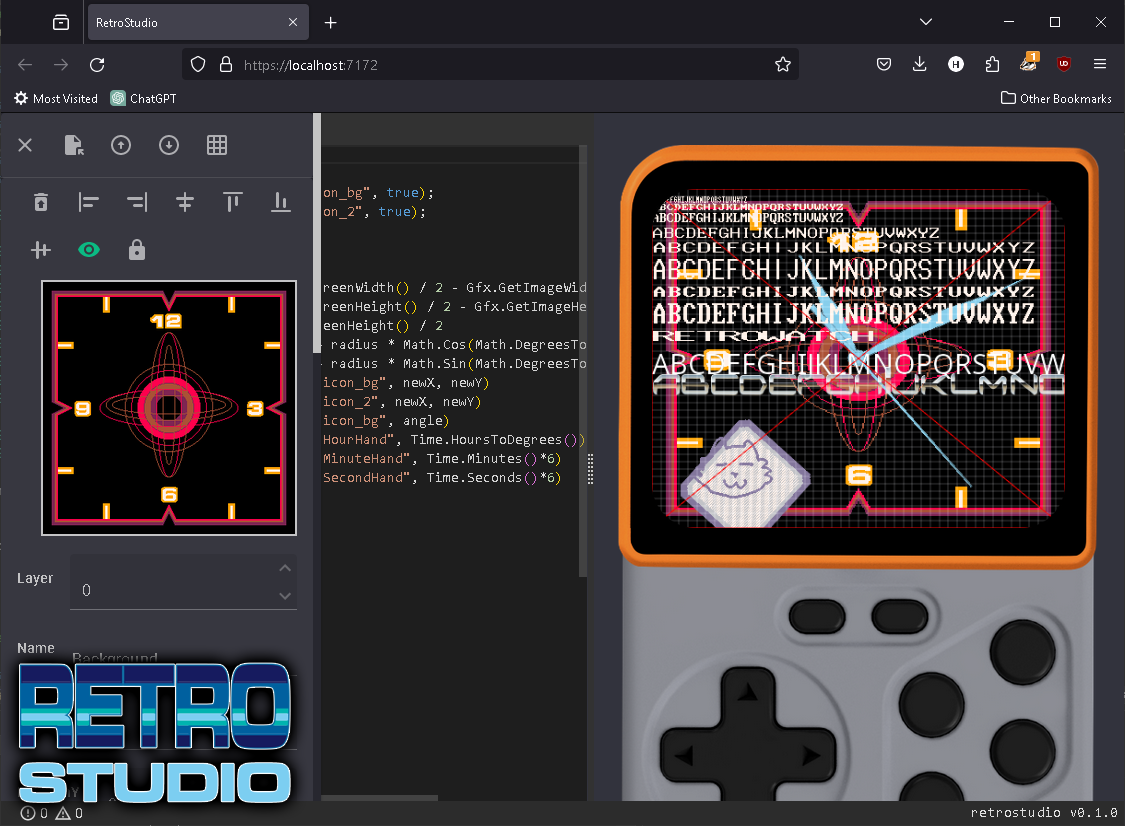
Retro Studio
Introducing Retro Studio our web IDE running an emulator of the Retro Watch.
Retro Studio will allow users to develop and test their own watch faces, games and applications before publishing them to the Retro Watch.
The back-end is written using Blazor Wasm and WebGL.
Stay tuned for more progress reports on this application!
Fully Funded!
We are fully funded and raised nearly $100k! It was an exciting month that's for sure. We are already well on our way to production and still a couple weeks away from the Kickstarter check clearing....having a lot of contacts willing to work on credit for this project put us a month ahead of schedule right out of the gate!
We will continue to accept preorders until we start our first production parts orders so if you missed out there is still a little time to get one.
Lobo and a Default Watch Face!
We're excited to announce that we have the amazing artist Lobo onboard who's going to be doing some design work including our default watch face. So keep an eye out for our future posts on that.
In the meantime we've been experimenting with the D/AVE 2D GPU on the DA14706 SoC for rendering a watch face. Take a look at the video below.
Please note this is just an experiment using the GPU on the RetroWatch and is not in any way indicative of the final design.
Hardware (FPGA) Assisted Emulation: Part 3
I am going to do the lazy thing and refer you to the Efinix getting started guides to get your tools set up. Since I'm one of one person who has a Retro Watch Devkit at the moment I think I can safely get away with this. But if I havn't filled this section in by the time you get yours feel free to call me on it!
[todo: tool setup, for now: use the Mipi devkiit guides here: https://www.efinixinc.com/products-devkits-triont20-mipi.html]
Okay, we are going to start with something very simple to get our feet wet. This is not meant to be a full blown FPGA and System Verilog tutorial but I'll try to explain as I go. I know, at some point, I am going to need a pixel counter that knows where its at in the render process. Ill keep track of the current render X and render Y in two 8 bit registers.
We are going to use these counters to generate our h_blank and v_blank output signals. This means our top level module will need a clock input and two outputs like follows:
module TopLevel(
    input clk,
    output reg h_blank,
    output reg v_blank
    );

endmodule
You can kind of think of a module as a function in programming in that it defines the input and the out put for the block of functionality. I tend to picture it as connectors you can use to wire one module to another.
For the moment, lets not worry about how to wire these signals to the outside world (its actually kind of annoying in the Efinix tool chain) and just assume we have a clock signal coming into our clk and two output signals routed to GPIOs (these signals leave the fpga and are connected to GPIOs on the main cpu).
Let's put together a quick pixel counter to generate the h_blank and v_blank signal.
Criteria:
We want a 256x256 pixel render. Not all of these pixels will be visible on the screen. Since our display is only 240 pixels wide we will set h_blank to 1 when the x counter is between 240 and 255. This will give us 16 pixels of time to do fun scan line effects later on. We will do the same thing for v_blank and give ourselves 16 full lines of blank time (a good time to update the tile graphics).
First, we declare two registers to hold our two counters, each one needs to go from 0 to 255 which is conveniently 8 bits. Since there is virtually no penalty for declaring a register of any width there are no predefined sizes (like int32_t or int8_t).
Next, we have a sequenction block of code which basically reads: Every time there is a positive edge to the clock: do the following. Hopefull the code is pretty self explanitory.
module TopLevel(
    input clk,
    output reg h_blank,
    output reg v_blank
    );

reg [7:0] pixel_x;
reg [7:0] pixel_y;

always @(posedge clk) begin

    pixel_x <= pixel_x + 1;

    if(pixel_x == 255) begin
        pixel_y <= pixel_y + 1;
    end

    h_blank <= pixel_x >= 240 ? 1 : 0;
    v_blank <= pixel_y >= 240 ? 1 : 0;
end

endmodule
Okay, we now have a pixel counter so lets take a quick moment to calculate our pixel clock because by default we have a 32Mhz clock comming in that is way too fast.
Now, we are not going to cheap out here and we are going for full 60fps gaming and the math is pretty straight forward:
256*256 pixels per frame times 60 frames per second. This results in a 3,932,160 Hz pixel clock.
To get that specific clock we are going to run our input clock (which is 32Mhz on the retro) through something called a phase locked loop (PLL) which will allow us to create pretty much any arbitrary clock frequency from any other. Here is much more indepth discussion on PLLs: https://www.digikey.com/en/maker/projects/introduction-to-fpga-part-9-phaselocked-loop-pll-and-glitches/2028ce62001b4cb69335f48e127fa366
[todo: insert screen shots that show how to do this on a Efinity software]
Okay, now our clock is set and we have v_blank and h_blank generating! But...how do we know its working? There are two options...first, we hook an oscope up to the pins and watch them toggle...that will be "truth" and often I do this just to make sure things are working like I think they are. But, more often we want to use the debugging capabilities built into the tool chain. Efinix doesn't have the most robust debugging tools but they are not too bad, basically you give up a little ram and logic in your design to create a virtual logic analyzer that will capture data sequencially and you can dump the captured data back to your computer and look at the waveforms. It takes some getting used to but is pretty powerful.
Again, i dont want to cloud this article with an Efinity how-to so check out the debugging documents in the link above while you wait for me to write that up (sorry, it just takes a lot of time to do all the screen captures). One thing to note about debugging on FPGAs: the debugger and the data you are watching actually become part of the design so to watch a new bus with your debugger requires you to recompile it and it consumes physcial ram on the device. On the relatively small FPGA inside retro you'll often have to be selective when using the debugger due to the resources it consumes.
[todo: add a screen shot of the debugger]
Let's do one final adjustment because we actually have a 320x320 display on the Retro that we normally drive for gaming. Generally, we want powers of two for just about everything on the FPGA whenever possible so lets change our render window to 512x512. The only other things we need to change is the blank signal math and the pixel clock settings (512x512*60hz = 15,728,640Hz).
module TopLevel(
    input clk,
    output reg h_blank,
    output reg v_blank
    );

reg [8:0] pixel_x;
reg [8:0] pixel_y;

always @(posedge clk) begin

    pixel_x <= pixel_x + 1;

    if(pixel_x == 511) begin
        pixel_y <= pixel_y + 1;
    end

    h_blank <= pixel_x >= 320 ? 1 : 0;
    v_blank <= pixel_y >= 320 ? 1 : 0;
end

endmodule
The above should look very familiar and only required a few small tweeks.
Okay, I think thats enough for one blog post. The next chapter will create an spi interface...dont worry, its really just a fancy shift register that we are going to add a simple command state machine to. Stay tuned for chapter 4!
PICO-8, DOOM and BLE!
Running tests on the DA14706 DevKit which has the Renesas ARM Cortex-M33F SoC we're using in the RetroWatch. Take a look at femto8 which is a PICO-8 fantasy console emulator as well as a port of DOOM both playable using a Bluetooth LE connected controller. So far performance is impressive and we're excited about bringing more games and emulators to the platform!